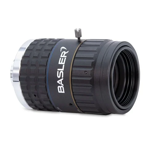
1. High-Resolution PCB Micro-Defect Inspection
Utilizes the 25 MP resolution capability and 2.71 µm pixel pitch compatibility to image dense circuit board layouts, allowing inspection software to locate micro-cracks and trace defects.
Problem SolvedResolves the challenge of identifying microscopic solder bridges and trace defects on modern high-density PCBs.
25 MP Resolution2.71 µm Pixel PitchSolder Joint Inspection
2. Automated Dimensional Metrology
Applies the low distortion characteristics and 50 mm focal length of the lens to achieve accurate, high-contrast measurements on machined metallic parts from a working distance of 200 mm or greater.
Problem SolvedEliminates measurement inaccuracies caused by optical distortion and vignetting across the edges of large 1.2" image sensors.
Low DistortionImage CircleMetrology
3. Semiconductor Wafer Alignment
Performs high-precision alignment verification of semiconductor wafers under visible spectrum light using a C-mount area scan camera.
Problem SolvedEnsures highly repeatable and crisp image capture of alignment fiducials at close working ranges.
C-mountVisible WavelengthFiducial Alignment