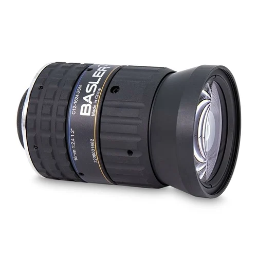
1. High-Precision PCB Inspection
Checking microscopic solder joints and component placement on dense printed circuit boards. The high-resolution 25 MP capability and 2.71 µm pixel pitch allow the machine vision system to capture fine micro-level details.
Problem SolvedPrevents false failures and undetected defects on complex PCBs where standard lenses lack the resolving power for tiny components.
25 MP ResolutionPCB InspectionPixel Pitch 2.71 µmFixed Focal Lens
2. Close-up Semiconductor Wafer Alignment
Aligning and inspecting semiconductor wafers at extremely close ranges. The low minimum working distance of 100 mm enables compact system integration without sacrificing image clarity.
Problem SolvedResolves space constraints in wafer manufacturing tools by allowing high-resolution imaging at short distances.
Minimum Working Distance 100 mmWafer InspectionManual IrisC-mount
3. High-Speed Packaging Thread Inspection
Inspecting physical defects and thread accuracy on bottling and packaging lines. Using a large 1.2" sensor format ensures minimal vignetting and consistent edge-to-edge resolution across the entire field of view.
Problem SolvedEliminates optical distortion at the image edges, ensuring that threads on the outer boundary of the object are measured as accurately as those in the center.
1.2" Sensor FormatLow VignettingLow DistortionPackaging Inspection