1. High-Resolution Solder Joint and PCB Component Inspection
Utilizing the lens in Automated Optical Inspection (AOI) systems for electronics manufacturing to scrutinize micro-components like 01005 capacitors and solder joint integrity at extremely close distances.
Problem SolvedMiniaturization in electronics makes manual inspection impossible. This lens provides the required optical clarity at a 0.03 m minimum object distance and 2.20 µm minimal pixel pitch to detect missing, misaligned, or poorly soldered microscopic components within compact machine footprint constraints.
Automated Optical Inspection12.00 MP resolution2.20 µm pixel pitch0.03 m M.O.D.
2. High-Speed Pharmaceutical Blister Pack and OCR/OCV Verification
Integration into pharmaceutical packaging lines to perform simultaneous Optical Character Recognition (OCR) on lot codes and defect inspection on blister packs using high-resolution industrial machine vision cameras.
Problem SolvedPharmaceutical lines require wide-angle, high-resolution imaging to capture an entire tray or blister pack at once while still resolving tiny printed text for compliance. The 8.0 mm focal length and 57.6° x 44.8° angle of view enable broad coverage, while the 12.00 MP optical class resolution prevents false negatives.
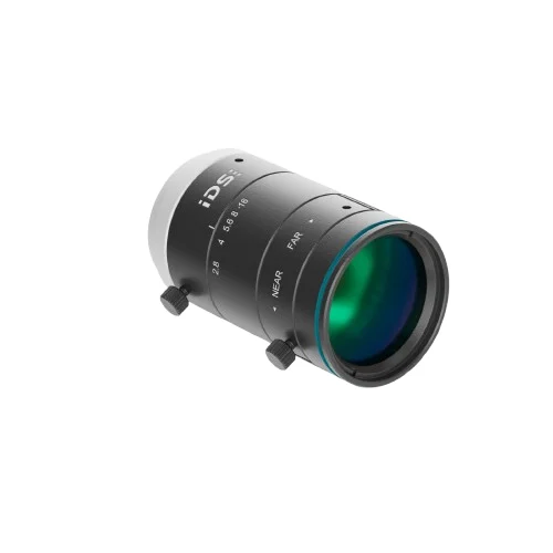
Optical Character Recognition8.0 mm focal length57.6° x 44.8° angle of view2/3" image circle
3. Inline Surface Defect Metrology for Precision Machined Parts
Deploying the lens on fixed industrial vision stations to detect micro-scratches, burrs, and dimensional inaccuracies on cast or machined mechanical components.
Problem SolvedEnsuring tight tolerances in precision manufacturing requires high-fidelity imaging. The lens's ability to resolve 2.20 µm pixel pitches allows for sub-millimeter defect detection, and the F2.8-16 aperture range provides flexible depth of field adjustments for parts with complex 3D topographies.
Surface Defect DetectionF2.8-16 aperture range2.20 µm pixel pitchMachine Vision Lens Metrology