1. High-Precision SMT and PCB Defect Inspection
Employed in automated optical inspection (AOI) systems for printed circuit boards, capturing highly detailed images of surface-mounted devices and solder joints from a close distance.
Problem SolvedDetects microscopic soldering flaws and misalignment of ultra-compact electronic components, replacing manual inspection and improving production throughput.
12.00 MP resolution2.20 µm pixel pitch0.10 m M.O.D.C-mount
2. Pharmaceutical Blister Pack Quality Control
Integrated into high-speed pharmaceutical packaging lines to perform real-time visual verification of pill presence, shape, and foil seal integrity on conveyor belts.
Problem SolvedEnsures absolute compliance in medication packaging by reliably identifying missing pills or defective seals across the entire package width without line slowdowns.
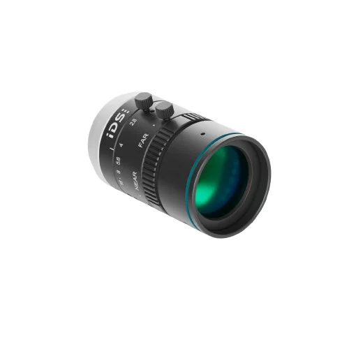
16.0 mm focal length30.8° x 23.3° angle of view2/3 inch image circle2.8-16 Aperture
3. Automotive Micro-Defect Surface Analysis
Mounted on robotic inspection arms to evaluate the surface finish and identify micro-scratches on precision-machined metal automotive components such as engine valves and bearings.
Problem SolvedPrevents premature component failure by catching sub-millimeter surface anomalies on complex metallic geometries that require adjustable depth of field and pristine optical clarity.
12.00 MP optical class2.8-16 aperture range14.89 mm back focal lengthC-mount